JDI: LTPS TFT와 NIR OPD를 이용한 휘어지는 생체인식(지정맥-지문인식) 솔루션 개발
Japan Display to boost profitability with new image sensor: CEO
https://mainichi.jp/english/articles/20200520/p2g/00m/0bu/103000c
Japan Display to boost profitability with new image sensor: CEO
http://www.ntech.t.u-tokyo.ac.jp/en/index.html
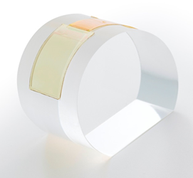
Conformable Thin Image Sensor
https://www.j-display.com/english/technology/jdisen/sensor02.html
Joint R&D With University of Tokyo Leads to World’s First Thin Image Sensor that Can Measure Fingerprints, Veins, and Pulse Waves
https://www.j-display.com/english/news/2020/20200121.html
A conformable imager for biometric authentication and vital sign measurement
https://www.nature.com/articles/s41928-019-0354-7
http://image-sensors-world.blogspot.com/2020/05/japan-display-inc-to-enter-image-sensor.html
JapanTimes, Mainichi: Japan Display Inc. (JDI) formed in 2012 through the merger of the display operations of Sony, Hitachi, and Toshiba announces its intention to enter image sensor business. The first product is 15um pixel-based bendable sensor developed with the University of Tokyo that can detect biometric information such as fingerprints and heart rate waves.
"We would like to foster our sensor products as a key pillar of our business that currently relies on the smartphone and the auto market," says JDI President Minoru Kikuoka. The company plans to introduce its image sensor products to the market in a few years, he added.
Japan Display Inc. (“JDI”) has developed a thin image sensor that integrated low-temperature polysilicon thin-film transistors with high mobility and high-sensitivity organic photodetectors. This image sensor can measure same time not only pulse wave distribution, which requires high-speed readout, but also biometric information, such as fingerprints and veins, which require high-resolution imaging.
Integration on a flexible substrate is also possible, the sensor is light weight and bendable.
As for biometric authentication, it is expected that the sensor will be applied to high security authentication systems to prevent imitations and impersonations by obtaining both biometric information (fingerprints and veins) and biometric signals (pulse waves).
Fingerprints and vein images have been processed to protect personal information.
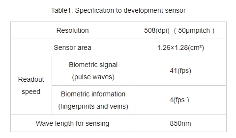
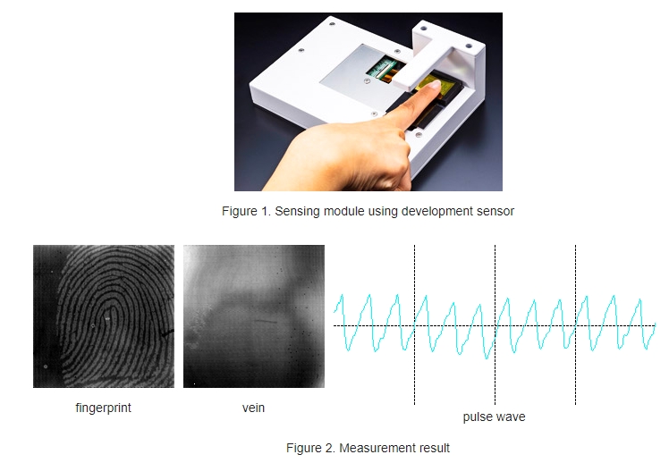
The development sensor, it is showed these Figure1,2 and Table1, through joint R&D with the Someya Group of the Department of Electric and Electronic Engineering, School of Engineering, University of Tokyo has received JST-Mirai Program Small Start Type (full-scale research ACCEL) (JPMJMI17FI) support from the Japan Science and Technology Agency (JST).
Reference :T. Yokota et al., “A conformable imager for biometric authentication and vital sign measurement,” Nature Electronics, DOI: 10.1038/s41928-019-0354-7, 2020.
Abstract
Flexible imagers can be placed in direct contact with a person’s skin, allowing vital signs to be monitored continuously. However, developing flexible imagers that offer both high definition and high speed has proved challenging. Here we show that a combination of polycrystalline silicon thin-film transistor readout circuits and organic photodiodes with high sensitivity in the near-infrared region can be used to create a conformable imager with a resolution of 508 pixels per inch, a speed of 41 frames per second and a total thickness of only 15 μm. The imager can read out a photocurrent of less than 10 pA with low noise, and can obtain static biometric signals, including images of fingerprints and veins, via soft contact with the skin. It can also be used to map a pulse wave, electronically selecting the best measurement location by analysing the area distribution.
Main
Many advances in biomedical measurements and medical diagnostic technologies have been realized through simultaneous improvement in the spatial resolution and time resolution of semiconductor imaging devices. Imaging elements in fluorescence microscopes1, endoscopes2 and X-ray devices3 are examples of this success. At the same time, the miniaturization of semiconductor devices has led to the development of imaging elements for wearable sensors that allow direct contact with the skin and thus continuous monitoring of vital signs4,5,6. To reduce the mechanical stress of such wearable sensors, the development of a flexible imager is of particular interest. High-speed (around milliseconds) flexible organic photodetectors (OPDs) have, for example, been created that can measure vital signs such as pulse waves7,8,9. In addition, large-scale flexible OPD matrices (with 254 pixels per inch (p.p.i.)) have been fabricated for measurements involving fingerprints and veins10,11,12. However, developing flexible imagers that simultaneously offer high definition and high speed is difficult because of the insufficient sensitivity of the flexible imagers created so far.
In this Article, we report a conformable imager with high resolution (508 p.p.i.), high speed (41 frames per second (f.p.s.)), and a total thickness of 15 μm. The conformable imager can read out a small photocurrent of less than 10 pA with low noise by combining low-temperature polycrystalline silicon (LTPS) thin-film transistor (TFT) readout circuits (backplane and complementary metal–oxide–semiconductor (CMOS) circuits) and an organic detector with high sensitivity in the near-infrared (NIR) region. The device can obtain static biometric signals, such as those from fingerprints and veins, via soft contact with the skin, and can also be used to map a pulse wave. Furthermore, the conformable imager can measure signals with extremely high accuracy to calibrate the displacement of the device electronically on the basis of fingerprint or vein feature points.
Structure of the conformable imager
Photographs of our conformable imager are shown in Fig. 1a,b. The system consists of an array of organic photodiodes for light detection, coupled to an active matrix backplane with LTPS TFTs for data addressing, and an analog front end (AFE) for data readout (Fig. 1c and Supplementary Fig. 1). The LTPS technology originally developed for high-resolution displays was utilized to manufacture the backplane designed for the array of OPDs. Figure 1b presents an image of the cell of the imager. The cell consists of LTPS TFTs and OPDs, which are connected through a via hole. The cell pitch, resolution, number of pixels and effective sensor area are 50 μm, 508 p.p.i., 252 × 256 cells and 12.6 × 12.8 mm2, respectively. The NIR OPD with maximum sensitivity at a wavelength of 850 nm shows good air stability because an inverted structure is used. When light is absorbed in the active layer of the organic photodiode, a photocurrent is generated by photoelectric conversion, and charges accumulate in the capacitor of each sensor. The accumulated charge is read out by the AFE. Depending on the amount of charge on the capacitor, the output voltage (Vout) of the comparator decreases from 0.75 V, which is the initial value of the signal line. The change in the output voltage is converted to a 10 bit digital signal. The conformable imager has mechanical flexibility because the AFE is integrated on a flexible printed circuit board (FPC). The dynamic range is 103 with an exposure time of 4.3 ms. The frame rate is 4.4 f.p.s. in the high-resolution mode that uses all the pixels (252 × 256).
Fig. 1: Conformable imager comprising LTPS TFTs and the NIR organic photodiode.
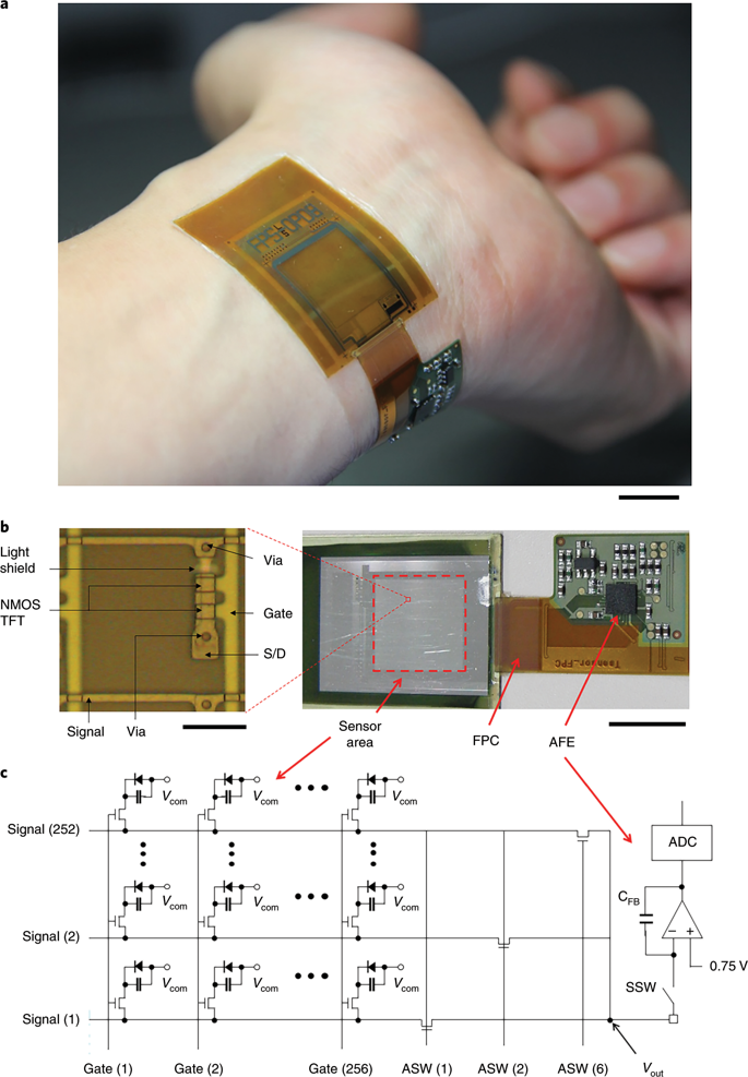
a, Photograph of an arm with a conformable imager attached. Scale bar, 1 cm. b, Photographs of the conformable imager. Scale bars, 20 μm (left) and 1 cm (right). c, Circuit diagram of the conformable imager. CFB, Vcom and SSW represent feedback capacitor, common voltage and series switch, respectively.
The fabrication process and structure are decribed in detail in the Methods and Supplementary Figs. 2–4. First, the LTPS TFT backplane was fabricated on a 10 µm-thick polyimide layer, which was coated on a glass substrate. Each cell consisted of a double-gate TFT comprising two serially connected n-type MOS (NMOS) TFTs with channel length of 4.5 μm, channel width of 2.5 μm and mobility of ~40 cm2 V−1 s−1. The double-gate structure was employed to improve the device yield13 and suppress the leakage current of the TFT (Supplementary Fig. 5). The driver circuit was formed using a CMOS design consisting of p-type MOS (PMOS) and NMOS TFTs with channel length of 4.5 μm and channel width of 3.5 μm (Supplementary Fig. 1). The mobilities of the PMOS and NMOS TFTs were both ~40 cm2 V−1 s−1. To fabricate the LTPS TFT, silicon oxide film (SiO), silicon nitride film (SiN), SiO and amorphous silicon film (a-Si) were first formed, then a-Si was crystallized via excimer laser annealing to form polycrystalline silicon (poly-Si). After forming poly-Si, source and drain regions of PMOS and NMOS were formed by doping with boron and phosphorus, then 70 nm-thick SiO and 250 nm-thick molybdenum-tungsten (MoW) were deposited as the gate dielectric and gate electrode, respectively. After fabricating the LTPS backplane, a 2 μm-thick planarization layer and a passivation layer were formed to integrate the OPD on top of the LTPS backplane. Via holes were formed using a dry etching system to connect the backplane and OPD.
An array of air-stable NIR organic photodiodes with inverted structure was formed on top of the backplane. The active layer, based on organic semiconductors, has good sensitivity at a wavelength of 850 nm. An indium tin oxide (ITO) electrode was used as a transparent electrode, and was connected to the backplane through the via holes. The surface of the ITO was coated with ZnO layers to adjust the workfunction of the electrode. Two different organic semiconductors—poly((2,5-bis(2-hexyldecyl)-2,3,5,6-tetrahydro-3,6-dioxopyrrolo(3,4-c)pyrrole-1,4-diyl)-alt-(3′,3′′-dimethyl-2,2′:5′,2′′-terthiophene)-5,5′′-diyl) (PMDPP3T)14 and STD-001 (conjugated polymer, Sumitomo Chemicals)—were used as the active layers to form two types of device. Each semiconductor was mixed with [6,6]-phenyl C61-butyric acid methyl ester (PC61BM) and spin-coated to form bulk heterostructures. Poly(3,4-ethylenedioxythiophene) doped with poly (4-styrenesulfonate) (PEDOT:PSS) and silver films were used as the top electrodes. The OPD was passivated with 1 μm-thick parylene and Cr/Au was evaporated for connection with the AFE. Finally, the organic imager was connected to the FPC with the AFE using an anisotropic conductive film. The AFE is a circuit that converts detected analog signals into digital signals, and consists of an amplifier circuit and a capacitor (see Methods). The device was peeled off the glass substrate in a laser liftoff process after completing all the manufacturing processes.
Characteristics of the conformable imager
The OPD was found to have a high sensitivity of 0.57 A W−1 when driven at −2 V at an NIR wavelength of 850 nm, as is commonly used for vein authentication; this is equivalent to the sensitivity of silicon photodiodes (0.5–0.7 A W−1). The characteristics of the organic photodiode are shown in Fig. 2a,b and Supplementary Fig. 6. The dark current density is 1.0 × 10⁻⁷ A cm−2 when driven at −2 V, and the photocurrent density when irradiated with NIR light at 850 nm with an output of 2.9 mW cm−2 is 1.7 × 10⁻³ A cm−2. The calculated on/off ratio for these values is ~1,000 (Fig. 2a and Supplementary Figs. 6 and 7). The external quantum efficiency (EQE) of our flexible organic photodiode is ~1.0 with a −2 V driving voltage at 850 nm (Supplementary Fig. 8). The detectivity of the OPD is 3.2 × 10¹¹ Jones (Fig. 2b). The EQE at a wavelength of 850 nm reaches 52% (Supplementary Fig. 9). The OPDs also demonstrated mechanical durability, air stability and high speed simultaneously: the change in current was ~10% after 500 cycles at a bending radius of 1.6 cm, the change in current was ~5% after storage in air for 20 days and the response time was less than 150 μs (Supplementary Figs. 10–12).
Fig. 2: Properties of the conformable imager.
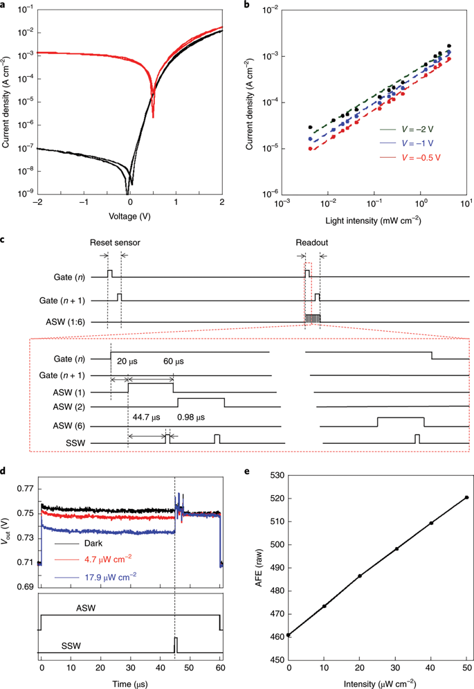
a, J–V characteristics of the single OPD in NIR light (red) and dark (black). b, Light-intensity-dependent photocurrent density of the OPD when irradiated by NIR light (850 nm). c, Readout method of the conformable imager. d, Change over time of the output signal (Vout). e, Light-intensity-dependent AFE signal. ASW, analog switch.
Almost all previous studies on NIR OPDs have reported high dark currents of over 10−5 A cm−2 and detectivities of ~1011 Jones6,15. Although flexible NIR organic photodiodes with low dark current have been reported, most show small EQEs (from 0.2 to 0.3)16,17,18. We have developed a flexible OPD that simultaneously exhibits high sensitivity and low dark current by optimizing the mixing ratio of the organic materials and the thickness of the active layer (Supplementary Figs. 13 and 14). With a thin active layer it is difficult to realize a lower dark current, while the EQE increases. With a thick active layer, the dark current can be reduced, but the EQE is reduced. In addition, the mixing ratio of PMDPP3T and PC61BM changes the photosensitivity: in our optimized structure the thickness of the active layer was 280 nm and the mixing ratio of PMDPP3T and PC61BM was 1:3.
LTPS backplane TFTs were used to achieve high resolution and high speed. The sensor area consisted of a high-resolution backplane TFT (with a cell pitch of 50 µm and resolution of 508 p.p.i.) and CMOS circuits. The LTPS backplane TFT can read out a cell at a high speed of 60 µs. These characteristics were realized using an LTPS with a mobility of 40 cm2 V−1 s−1, which is higher than for organic transistors19, oxide transistors11 and amorphous Si transistors20, all of which have mobilities in the range of ~1–10 cm2 V−1 s−1. The large mobility of the TFTs contributes to reducing the readout time. In a simulation, the response time of the waveform at the typical mobility of LTPS (40 cm2 V−1 s−1) was as small as 1 μs (Supplementary Fig. 15). Due to this small response time, our imager can read out one cell at a high speed of 60 µs. The LTPS CMOS circuits can be formed by integrating PMOS and NMOS TFTs, which can be realized easily by changing the doping material. Moreover, the LTPS TFTs have a high on/off ratio of 107, which is higher than for organic transistors21 or a-Si transistors22 (on–off ratios of ~104–106). The characteristics of the LTPS TFTs integrated in CMOS circuits are shown in Supplementary Fig. 16. The PMOS and NMOS TFTs have mobilities of 40 and 40 cm2 V−1 s−1, threshold voltages of −2.60 and 1.87 V, respectively, and an on/off ratio of 107. The NMOS TFTs used in the backplane are shown in Supplementary Fig. 17. The threshold voltage, mobility and on/off ratio are 1.8 V, 47.9 cm2 V−1 s−1 and 107, respectively. A sufficiently low off current and high on current, comparable with the dark current and photocurrent of organic photodiodes, are required in a backplane TFT. The changes in the current of the LTPS TFT were as small as 3% after complete integration with OPDs (Supplementary Fig. 18).
In previous reports on flexible NIR OPDs, the photocurrent was weak (~pA level) because of the low sensitivity of these devices15. If the sensing area of an OPD is reduced by increasing the resolution, the photocurrent is further reduced; moreover, the charge must be accumulated in the capacitor for a long time, so readout speed is sacrificed. On the other hand, to read out the photocurrent with high speed, it is necessary to increase the light-receiving area of the detector and sacrifice resolution. In our conformable imager, by combining the high resolution and high speed of the LTPS TFT (backplane and CMOS circuits) and the high sensitivity of the OPD, the integrated device can read out low-intensity NIR light signals at high speed. Figure 2c presents the readout method for the imager. First, the sensor capacitor is reset before light is incident on the sensor area. Next, the reference potential of 0.75 V is written in each sensor capacitor and signal line by opening a gate by line scanning. Finally, the charge of each sensor capacitance is read out by opening a gate, line by line. The amount of charge depends on the light intensity and the irradiation time. Figure 2d shows the change in the output signal (Vout) over time when NIR light is incident on the sensor area for 4.3 ms. After turning on the analog switches (ASWs), Vout immediately decreases and, as the irradiation intensity increases, the voltage change increases. The integrated device can detect low-intensity NIR at 4.7 µW cm−2. The light intensity dependence of the output signal after connecting the AFE is shown in Fig. 2e. The output signal shows linearity below 50 µW cm−2, and the imager was also able to detect a low intensity of 10 µW cm−2 before connecting the AFE. We measured the output signal of the AFE when irradiated with NIR light of 0 and 10 µW cm−2 (Supplementary Fig. 19). A difference process was performed to reduce any device variation. Following the difference process, the variation width was reduced from 50 to 20 (see Methods and Supplementary Fig. 19).
Imaging of static biometric signals
We confirmed the imaging resolution of the conformable imager to be 508 p.p.i. Figure 3a shows the imaging result obtained from a resolution chart which has 15 lines with 50 µm linewidth and linespace. The square-wave response function (SWRF) of our conformable imager was evaluated using the Fig. 3a chart (Supplementary Fig. 20). The SWRF was 0.76 with a spatial frequency of 10 line pairs per millimetre (lp mm−1). The captured image has 15 lines in the finest pattern area. In addition, there were no defects in any of the 252 × 256 cells, and high uniformity was realized for the conformable imager.
Fig. 3: Biometric imaging.
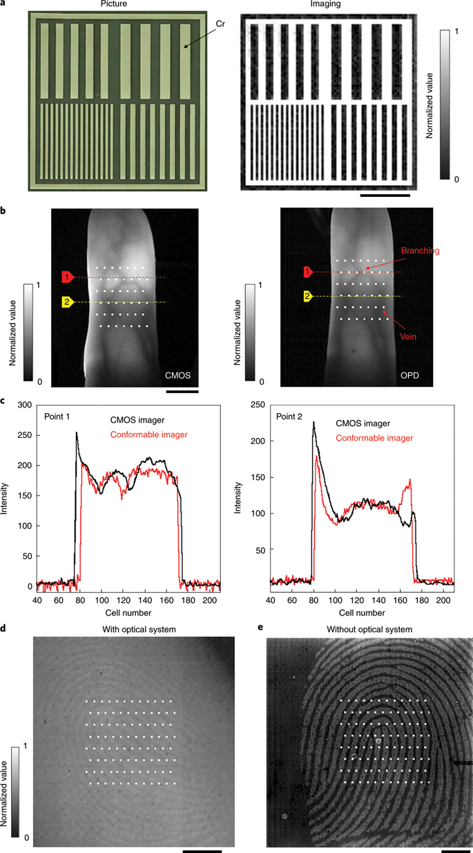
a, Resolution test of the conformable imager. The left and right figures represent the picture and imaging results of the resolution chart, respectively. Scale bar, 1 mm. b, Imaging of a finger vein. The left and right images were taken by CMOS and conformable imagers, respectively. A two-dimensional (2D) array of white dots has been added to the images to protect personal information from biometric identification. The dots are 0.3 mm square and the horizontal and vertical pitch are 0.9 and 1.5 mm, respectively. Scale bar, 5 mm. c, Signal intensity distributions at two locations of the vein (shown in b), taken by the CMOS imager (black) and the conformable imager (red). d, Imaging of a fingerprint taken by a conformable imager with the optical system. A 2D array of white dots has been added to the image to protect personal information. The dots are 0.05 mm square and the horizontal and vertical pitch are 0.15 and 0.25 mm, respectively. Scale bar, 1 mm. e, Imaging of a fingerprint taken by a conformable imager without the optical system. A 2D array of white dots has been added to the image to protect personal information. The dots are 0.07 mm square and the horizontal and vertical pitch are 0.21 and 0.35 mm, respectively. Scale bar, 1 mm.
This high resolution, with no defects and high uniformity, is necessary for feature quantity extraction in biometric authentication using a fingerprint or vein. Figure 3b shows the imaging of a finger vein using the transmission mode and optical system (for details see Methods and Supplementary Fig. 21). The imaged vein has features such as a vein branch point, branching angle and number of veins, which are important factors for vein authentication.
Figure 3c shows the signal intensity distribution at locations of the vein at which the image was captured by the CMOS imager and the conformable imager. Although the CMOS imager shows ~70% lower noise level than our imager, the contrast difference at the vein is less than 5%. We thus confirm that the conformable imager has high image quality equivalent to that of conventional CMOS imagers. To demonstrate the advantages of our imager, namely its mechanical flexibility, high speed and high definition, we integrated a flexible louvre and NIR light-emitting diode (LED) with the imager and acquired an image of the wrist vein without additional optical components (Supplementary Fig. 22). The contrast of the vein and other locations was ~1.5.
Next, a fingerprint was captured in reflectance mode using the optical system (Fig. 3d and Supplementary Fig. 23). The image of the fingerprint has important features for biometric authentication—number of ridges (level 1 features), endpoints and branching points (level 2 features). Furthermore, the digital output difference between ridges and valleys is ~200, which is sufficient for biometric authentication when using image processing methods such as binary conversion. In addition, the conformable imager meets the standard of 508 p.p.i. that is recommended in ISO/IEC 19794-2 for fingerprint authentication.
In a unique feature of the conformable imager, fingerprints can be captured by directly attaching the conformable imager to the skin, without an optical system such as a lens (Supplementary Fig. 24). Figure 3e presents a fingerprint image obtained without an optical system. The fingerprint image shows the number of ridges, the branch point and the end point, but also the position of the sweat gland (level 3 features), which is needed to realize high-accuracy authentication23. The conformable imager can obtain a very clear fingerprint without an optical system, and the entire system can be made to be flexible. Interestingly, if a conductive film is placed between the fingers and the conformable imager, fingerprints cannot be captured (Supplementary Fig. 25a). Furthermore, it should be noted that we acquired the fingerprint image under dark conditions without light illumination (Supplementary Fig. 25b). This means that fingerprints could be captured, not only using a conventional optical system, but also with an electrostatic capacitive method.
Detection of photoplethysmogram signals
The conformable imager can measure not only static biometric parameters but also dynamic parameters such as pulse waves. Supplementary Fig. 26 shows a pulse wave measured by the conformable imager. The red and black lines represent the pulse wave, measured respectively by the imager and an existing commercial instrument (IWS920-DEV, Tokyo Devices, a finger-clip-type pulse meter that uses a transmission method). Both devices show the same heart rate of 77 beats per minute. The average time difference in the peak position of the pulse was 30 ms when compared to the conventional device.
The conformable imager can capture the entire area of photoplethysmogram (PPG) signals at 41 f.p.s. Figure 4a shows the mapping of the pulse wave intensity using the conformable imager. On analysing the mapping of the pulse wave intensity, the minimum point has been reduced to ~40% of the maximum point. It is interesting to note that the pulse intensity has changed considerably in the ridge and valley lines of the fingerprint (Fig. 4a). The pulse intensity variation is caused by the difference in in-coupling and out-coupling. This is because the distance between the imager and finger changes in the ridge and valley lines. Thus, by measuring the pulse wave at multiple points, high-quality measurements can be obtained by selecting a position that provides stronger signal intensity. Moreover, the conformable imager can simultaneously measure the pulse wave and feature points such as finger shapes and fingerprints. Therefore, it is possible to track the same point before and after the finger moves. Figure 4a shows the mapping of the pulse wave intensity after moving the finger. The finger has moved by five cells from position A. Therefore, the intensity mapping of the pulse wave has also shifted, following the finger movement (Fig. 4a,b). Without the displacement prevention function, the intensity decreased to 50%, but it could be reduced to only 20% with the displacement prevention function (Fig. 4c). The intensity change of 20% depends on how the finger is placed on the conformable imager system; hence, this does not mean that the 20% change in the intensity is limited by the performance of the displacement prevention function.
Fig. 4: Analysis of the PPG signal.
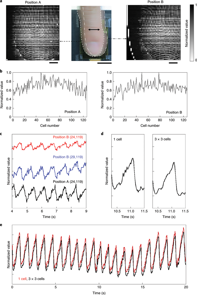
a, PPG signal intensity mapping of the finger. Scale bars, 2 mm, 1 cm, 2 mm (left to right). The dashed line and dash-dotted line indicate position A and position B, respectively. b, The PPG signal intensity at the vertical white lines in a. c, The PPG signal for different cells. The (24,119) cell of position A and the (29,119) cell of position B detect the PPG signal at the same place on the finger. d, The PPG signal of one cell (left) and the average of nine cells (right). e, Long-term measurements of the PPG signal. Red and black lines represent the PPG signal of one cell and the average of nine cells, respectively.
The conformable imager was not only high-resolution, but the effective area can be freely changed by measuring multiple points of cells collectively. Figure 4d,e shows the measurements results of the pulse wave obtained by changing the size of the light-receiving area. The red and black lines represent the pulse wave with one cell and nine cells (3 × 3) cells, respectively. The noise level was reduced and the signal-to-noise ratio (SNR) was improved from 5 to 20 dB by increasing the light-receiving area. The SNR is almost the same for an array size of 3 × 3 or more.
Conclusions
Our conformable imager can capture images of both fingerprints and veins. For fingerprint authentication, the authentication ratio decreases as a result of skin wounds24, while the equivalent error rate improves by 40–60% when performing authentication using a fingerprint and vein compared with the case of performing authentication with either a fingerprint or a vein25. Therefore, it is expected that a high authentication rate can be realized by performing biometric authentication using the conformable imager.
Furthermore, the conformable imager can measure biosignals such as pulse waves as well as biometric parameters such as fingerprints and veins. Conventional devices have separate authentication systems and devices that measure biological signals. However, our conformable imager can obtain biometric information and measure biosignals simultaneously. In addition, it is expected that ‘impersonation’ by mimicking biometric information26, which is a problem in conventional authentication systems, can be prevented by measuring vital signs at the same time as authentication.
High-precision monitoring of pulse waves, and their analysis with appropriate algorithms, can elucidate important biological parameters such as blood pressure27, blood oxygen concentration28 and thrombus location29. Our conformable imagers could be used to monitor such signals during daily life. Furthermore, as the conformable imager can be fixed to any part of the body, it could also be possible to detect cerebral thrombosis30 and intracerebral haemorrhage31 by placing the device near the brain.
The fabrication of high-performance flexible NIR OPDs was critical to realize a conformable imaging system that enables continuous high-precision, stress-free health monitoring. For example, the EQE of our flexible NIR OPDs is 52%, while the maximum EQE for the previously reported flexible OPDs was only 30% at 850 nm (ref. 8). Furthermore, the high performance seen in discrete devices has, with our approach, been reproduced after integration. This was possible due to use of state-of-the-art microfabrication techniques, including our low-temperature process and encapsulation technique, as the silicon active matrix does not deteriorate during the liquid process (Supplementary Fig. 27).
Methods
Materials
PC61BM and PMDPP3T were purchased from Solenne BV Corporation and Luminescence Technology Corp., respectively, and STD-001 was supplied by Sumitomo Chemical Company. Zinc acetate dehydrate was purchased from Wako Pure Chemical Industries and PEDOT:PSS (Clevios Al 4083) was purchased from Heraeus Deutschland.
Fabrication of the conformable imager system
LTPS TFT backplane
A 10 μm-thick layer of polyimide was formed on the glass substrate and thermally annealed at 500 °C for 30 min, then a 100 nm-thick SiO film was deposited as an undercoat layer via plasma-enhanced chemical vapour deposition (PECVD) to prevent damage to the polyimide layer during the subsequent SiN and metal deposition. For the light shield layer of the LTPS TFT, a 50 nm-thick layer of MoW was patterned using the sputtering method. Layers of SiO, SiN film, SiO and a-Si film were deposited, in order, via PECVD. The a-Si layer was crystallized via excimer laser annealing to obtain poly-Si after dehydrogenation annealing, and the poly-Si was patterned into an island shape. Boron and phosphorus were ion-doped into the electrode portions of the PMOS TFT and NMOS TFT. A 70 nm-thick SiO film was formed as a gate dielectric by PECVD, then a 250 nm-thick MoW layer was patterned as a gate electrode. To form a lightly doped drain (LDD), phosphorus ions were implanted. Contact holes were opened by dry etching. The mobility between the NMOS TFT and PMOS TFT was adjusted by changing the impurity dose amount in the LDD, while also changing the length of the LDD from 1 to 2 μm. The source and drain electrodes were formed by depositing Ti/Al/Ti, then a 2 µm-thick planarization layer was deposited and a 50 nm-thick ITO electrode was patterned as the transparent electrode of the sensor. Finally, the substrate was cut to separate each chip. Thanks to the thin flexible substrate, the LTPS TFTs were functional at a bending radius of 5 mm (ref. 32).
OPD
The surface of the chip was treated with oxygen plasma (10 s at 300 W), then a 20 nm-thick ZnO layer was formed by spin-coating (5,000 r.p.m. for 30 s). A ZnO precursor solution was prepared by dissolving zinc acetate dehydrate (0.5 g) and ethanolamine (0.16 ml) in 2-methoxyethanol (5 ml). The substrate was annealed in air at 180 °C for 30 min. The active layer was obtained from a PMDPP3T and PC61BM solution with a weight ratio of 1:3 in mixed solvent (chloroform and o-dichlorobenzene with a volume ratio of 4:1) to yield a total of 20 g l−1. The solution was deposited by spin-coating at 250 r.p.m. for 4 min to form the thicker active layer (the thickness of the active layer was ~280 nm). STD-001 and PC61BM solution with a weight ratio of 2:3 in o-dichlorobenzene was used to yield a total of 50 g l−1 to form the active layer. The solution was deposited by spin-coating at 625 r.p.m. for 4 min, followed by annealing in nitrogen at 100 °C for 10 min. After forming the active layer, a 10 nm-thick layer of PEDOT:PSS was spin-coated at 2,000 r.p.m. for 30 s from an isopropanol solution (15% in volume) and annealed on an 80 °C hot plate for 5 min in a nitrogen atmosphere. Finally, 80 nm-thick Ag was deposited as an electrode and a 1 μm-thick parylene layer was coated via CVD as a passivation layer.
Integration process
A flexible cable was laminated to the device using anisotropic conductive film tape. After connecting the flexible cable, the device was delaminated from the supporting glass substrate via a laser liftoff method. The OPD current changed by less than 10% after the liftoff process (Supplementary Fig. 27).
Design of circuits
Supplementary Fig. 1 presents a circuit block diagram of our set-up. The number of pixels was 252 × 256 cells. Each cell consisted of a TFT, a pixel electrode and a common electrode. The OPD was formed between the pixel electrode and the common electrode. To control each row in the cell, a gate driver circuit was fabricated using CMOS TFTs on the left side of the sensor area. The gate driver consisted of shift resistors (S/R) and buffer circuits. The operation mode could be switched to choose between driving the gate lines either one by one or two at a time, by changing the start vertical (STV), clock (CK), output enable 1 and 2 (OE1 and OE2) signals (Supplementary Fig. 1). The reset (RST)1 signal was used to reset the shift resistor. A selector was fabricated on the bottom side of the sensor area that consisted of 42 sets of circuits that convert six inputs to one output. The six control signals, namely ASW (1), ASW (2), ASW (3), ASW (4), ASW (5) and ASW (6), were input to the selector. By changing these signals, the operation mode could be selected such that the signal lines (Sig) were connected either one by one or several lines at a time. The potential of the common electrode was set to −1.25 V (Vcom). The potential of the pixel electrode was periodically reset to 0.75 V, which was the intermediate potential of the comparator in the AFE, and then the potential was reduced by the photocurrent of the OPD. The change in charge in each cell was detected by connecting the gate line, an ASW switch and an SSW switch. The charge value was converted to a voltage by capacitor (CFB), and then the voltage was digitized by the analog-to-digital converter to make it raw data. The power consumption of the imaging system was ~1.8 W
Processing
The output signals of the AFE (AFEdark) were measured under dark conditions (for reference) then the output signal of the AFE (AFEsignal). To reduce the device variation of the cells, we performed the differential process AFEsignal − AFEdark.
Electrical characterization of the conformable imager system
I–V characterizations of LTPS TFTs
All electrical characteristics were measured using a semiconductor device analyser (B1500A, Agilent Technology).
J–V characterizations of the organic photodiode
To evaluate the organic photodiode we carried out measurements on the standalone device, which had an area of 4 mm2. All electrical characteristics were measured using a semiconductor device analyser (B1500A, Agilent Technology) or a Keithley 2400 source measure unit. EQE values under varying voltages were measured using a Hyper Monolight SM-250 system (Bunkoh-Keiki). The light intensity was modulated using a series of neutral density filters (Newport Optics). The EQE can exceed 1 when a voltage is applied to the OPD, but it cannot do so with no voltage bias33. The detectivity (D*) could be evaluated from the responsivity and noise current. The noise current mainly arose from the shot noise from the dark current34. D* could be estimated with the equation
D∗=R2qID−−−−√D∗=R2qID
where R is the responsivity, q is the electron charge and ID is the dark current.
Characterization of the conformable imager
All electrical characteristics were measured using a semiconductor device analyser (B1500A, Agilent Technology). To measure the photoresponse of the conformable imager, the substrate was exposed to NIR light (IHM108/114IR-850, IMAC Co.). The intensity of the NIR light was measured with an Optical Power Meter 3664 (Hioki E.E. Corporation). The total thickness of the conformable imager was just 15 µm and it showed good flexibility due its thickness. Flexibility is related to the bending strain ε∼D2Rε∼D2R (ε, strain; R, bending radius; D, thickness), so, to prevent mechanical failure of the devices, we reduced the thickness of the substrate. Accordingly, the bending stiffness of the thin-film imager (composed of non-elastic materials) was reduced by decreasing the thickness.
Driving method of the conformable system
Supplementary Fig. 28 shows the timing chart for the control signals (STV, CK, OE1, OE2, ASW (1), ASW (2), …, ASW (6), SSW). Case A was a high-resolution mode that read all the cells, one by one. Case B shows examples in which two gate lines were driven at the same time, and a plurality of signal lines connected to each channel of the AFE were driven at the same time. Moreover, in case B, two gate lines were simultaneously opened and closed, and ASWs (1) to (6) were simultaneously opened and closed; this means that a total of 12 cells were collectively driven. In case C, ASWs (1) to (6) were simultaneously opened and closed, which means that a total of six cells were collectively driven.
Measurement of biometrics signals
Measurement of the finger vein (with an optical system)
The measurement set-up is shown in Supplementary Fig. 21. The vein was observed using transmitted light. The optical lens (Canon Macro Lenz EF-S 60 mm) was placed on the imager and its focus was adjusted. The distance between the finger and lens was 200 mm. The vein was imaged using all sensors (252 × 256). An LED with a wavelength of 850 nm (OSRAM, SFH4052) was placed on the top of the finger. The light intensity of the LED was 51 µW cm−2 at a distance of 330 mm from the LED and 520 µW cm−2 at 100 mm from the LED. A CMOS imager (DHT Corporation, 22K9HE-EX) was used as a reference.
Measurement of the wrist vein (without an optical system)
The measurement set-up is shown in Supplementary Fig. 22. The vein was observed using reflected light. View control film (Shin-Etsu Polymer Co., N-VCF1003000-PC100-X) was used as a flexible louvre to transmit only the vertical component of the light transmitted or reflected from the finger or wrist. The vein was imaged using all sensors (126 × 128). Six LEDs with a wavelength of 850 nm (VSMY12850) were placed on the side of the imager. The light intensity of the LEDs was 200 µW cm−2 at a distance of 100 mm from the LEDs.
Measurement of a fingerprint with an optical system
The measurement set-up is shown in Supplementary Fig. 23. The fingerprint was observed using reflective light. The optical lens (Canon Macro Lenz EF-S 60 mm) was placed on the imager system and its focus was adjusted. The distance between the finger and lens was 150 mm. The fingerprint was imaged using all sensors (252 × 256). An LED (JGN-5306X) with a wavelength of 850 nm was placed on the side of the lens. The light intensity of the LEDs was 590 µW cm−2 at a distance of 100 mm from the LED.
Measurement of a fingerprint without an optical system
The measurement set-up is shown in Supplementary Fig. 24. The finger was directly attached to the sensor and LEDs (JGN-5306X) with a wavelength of 850 nm were placed 110 mm above the finger. The light intensity of the LEDs was 256 µW cm−2 at a distance of 125 mm from the LED. The fingerprint was imaged using all sensors (252 × 256).
Measurement of the pulse wave
The measurement set-up is shown in Supplementary Fig. 24. The finger was directly attached to the sensor and LEDs (JGN-5306X) with a wavelength of 850 nm were placed 110 mm above the finger. The light intensity of the LEDs was 70 µW cm−2 at a distance of 125 mm from the LED. The fingerprint was imaged using all sensors (42 × 128). The SNR of the signal was calculated by
SNR=20×log(△IPPG/△INoise)SNR=20×log(△IPPG/△INoise)
where ΔIPPG is the amplitude of the PPG signal and ΔINoise is the amplitude of the noise signal.
The study protocol was thoroughly reviewed and approved by the ethical committee of the University of Tokyo (approval no. KE18-41).
Reporting Summary
Further information on research design is available in the Nature Research Reporting Summary linked to this article.
Data availability
The data that support the findings of this study are available from the corresponding authors upon request.
References
-
1.
Bailey, B., Farkas, D. L., Taylor, D. L. & Lanni, F. Enhancement of axial resolution in fluorescence microscopy by standing-wave excitation. Nature 366, 44–48 (1993).
-
2.
Herz, P. R. et al. Micromotor endoscope catheter for in vivo, ultrahigh-resolution optical coherence tomography. Opt. Lett. 29, 2261–2263 (2004).
p.s
기존에는 정전용량식으로 개발해서 관심이 떨어졌는데 이제 광학식으로 발전
JDI는 장기적으로 생존이 불가능해 보이는 것이 가장 문제.
Development of Flexible Fingerprint Sensor
https://www.j-display.com/english/news/2019/20190509.html
Capacitive-type flexible fingerprint sensor

Smart card usage

Commence mass production of capacitance type glass fingerprint sensor
https://www.j-display.com/english/news/2018/20181220.html
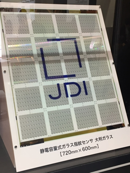
Fingerprint sensors built onto LTPS glass substrate
Capacitance type glass fingerprint sensor module
http://www.ntech.t.u-tokyo.ac.jp/en/index.html

https://twitter.com/iamritu/status/1263265269478195200
Q2. question: study LED lights & photodiodes used to get photoplethysmogram (PPG) (pulse estimation) Time between PPG signal peaks (intervals between pulses)create a tachogram & if abnormal pt notified & led to virtual visit/ECG patch (“ePatch”)but had low ppv #TelemedNow

'지문인식 업계, 시장 동향' 카테고리의 다른 글
| CINNO: 올해 FoD 출하량 273m 예상, Omdia 4억개 이상 예상과 차이 보여 (0) | 2020.06.13 |
|---|---|
| 카운터포인트: 작년 스마트폰 UD지문센서 침투율 14% (0) | 2020.06.13 |
| 이스라엘 Tower 반도체, 2020 1분기 결과 Q&A중에서 생체인식 관련 (0) | 2020.06.13 |
| Omdia: 작년 FoD시장 2억 2천 8백만대, 올해 4억개 이상, CIS기반 솔루션 88% 예상 (0) | 2020.06.13 |
| 3M: LCD 모바일 장치용 전화면 지문,얼굴,제스처 인식이 모두 가능한 솔루션 NITS 개발 (0) | 2020.06.13 |


