A High‐Resolution Thin‐Film Fingerprint Sensor Using a Printed Organic Photodetector
A High‐Resolution Thin‐Film Fingerprint Sensor Using a Printed Organic Photodetector
https://onlinelibrary.wiley.com/doi/full/10.1002/admt.201900651
Abstract
Organic photodetectors (OPDs) have attracted much attention in recent years, due to their promise in large‐area light sensing applications. Here, high‐resolution slot‐die‐coated large‐area bulk heterojunction organic photodiode (OPD) arrays are reported. The OPD uses a novel electron transport layer, indium gallium zinc oxide in combination with a molybdenum oxide top‐electrode. Together, these effectively reduce dark current densities to very low levels of ≈10−7 mA cm−2 at −2 V. The OPDs show linear behavior in a wide range of light intensities and high detectivity values under reverse bias conditions. When coated on a 508 ppi TFT backplane, a high‐quality optical fingerprint scanner capable of imaging in reflection is realized. The optical and electrical properties of the fingerprint sensor are characterized and high‐resolution fingerprint images are obtained.
With organic photodetector (OPD) technology growing in maturity, new imaging applications emerge.1, 2 For instance, smartphone manufacturers have been moving toward a full‐face display, thereby eliminating the space for the fingerprint sensors in the home button. An elegant solution would be the implementation of a thin‐film fingerprint sensor within the display area. Ultrasonic and thermal fingerprint sensors have been developed3, 4 but possess some drawbacks; ultrasonic sensors have a high cost for large‐area display applications and the images of thermal sensors have a very short lifetime.5 An alternative would be to use an optical fingerprint sensor using solution‐processed OPDs. OPD‐based sensors are very good candidates for this purpose as their solution processability, coupled with low process temperatures, allows for cost‐effective fabrication of large‐area (≫cm2) photodetector arrays on thin, plastic substrates.6-10 Moreover, these devices show high photogeneration sensitivities, fast response times, and their absorption can be tuned from the ultraviolet to the near‐infrared.1, 11 However, it is not easy to process large‐area, homogeneous thin OPD films by conventional coating techniques, such as spin‐coating. Using slot‐die coating of the active organic photodetector materials, we have developed a cost‐effective, scalable photodetector array technology. We demonstrate its use in a high‐resolution fingerprint detector with a thin form factor that ultimately would allow users to securely unlock their phone or open user‐specific apps by touching anywhere on the display screen.
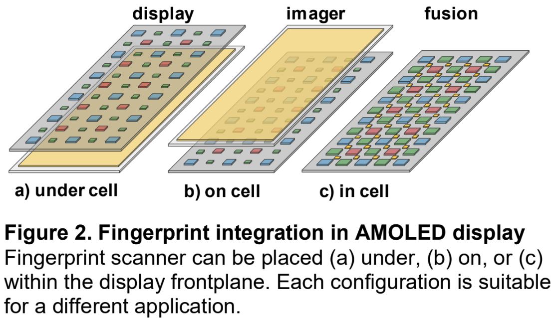
The fingerprint scanner is based on three main building blocks (Figure 1a for a schematic of the fingerprint scanner, Figure 1b for the circuit diagram, and Figure S1, Supporting Information, for a full stack cross section). The backplane is a dual‐gate self‐aligned oxide thin‐film transistor (DG‐SA TFT) array, described and characterized elsewhere.12 The second (bottom) gate is typically used to increase the transistor current for a given geometry and voltage. Here, it also acts as a light shield of the oxide semiconductor in case of backside exposure, thereby increasing device stability.13 The DG‐SA TFT exhibits a low off‐current with values below 1 pA, lower than the off‐currents of amorphous and low‐temperature polycrystalline silicon transistors. This is due to the large bandgap of IGZO (≈3 eV) that results in a low leakage current. The field‐effect mobility of our TFTs is 15 and 16 cm2 V−1 s−1 for the top and bottom gate operation, respectively. In so‐called dual gate mode, that is, V g top = V g bottom, the effective mobility is equivalent to 35 cm2 V−1 s−1. The values can be compared to a‐Si TFTs (≈1 cm2 V−1 s−1) and LTPS TFTs (≈100 cm2 V−1 s−1). The frontplane consists of organic photodiodes (OPDs). The technology is based on a bulk heterojunction (BHJ) structure of a p‐type (donor) polymer, poly[N‐9′‐heptadecanyl‐2,7‐carbazole‐alt ‐5,5‐(4′,7′‐di‐2‐thienyl‐2′,1′,3′‐benzothiadiazole)], PCDTBT, and an n‐type (acceptor) fullerene, 6,6‐phenyl‐C61‐butyric acid methyl ester, PCBM. The blend is deposited by slot‐die coating, resulting in a 280 nm film. Semitransparent IGZO (bottom) and MoOx/Ag (top) electrodes are used.
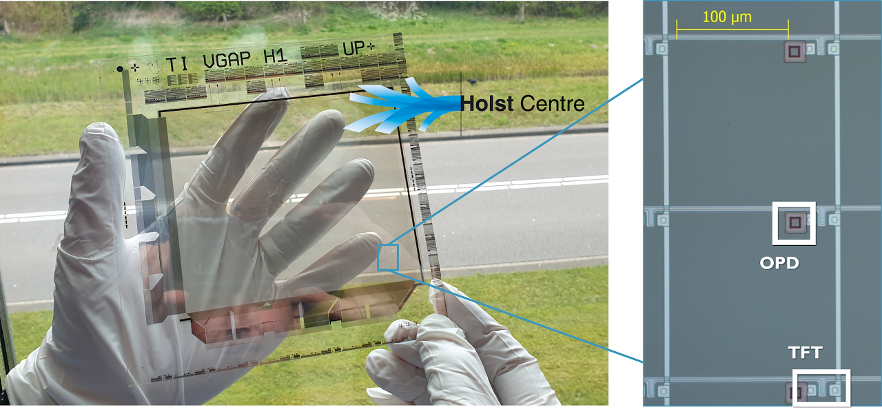
The a‐IGZO is deposited on top of an opaque MoCr layer. This is done to prevent direct detection from the backlight, so only light that is reflected from objects on top of the imager array is measured by the OPD. The sensor is coupled with an optically transparent thin‐film encapsulation to avoid moisture ingress that degrades the OPD materials.14 The fabrication processes are compatible with flat panel display manufacturing lines. Details on the step‐by‐step fabrication can be found in the Experimental Section. A photograph of the full device can be seen in Figure 1c. Gate driver and readout IC connections are bonded to the sensor platform. The optical imager technology has been scaled up to larger areas.15
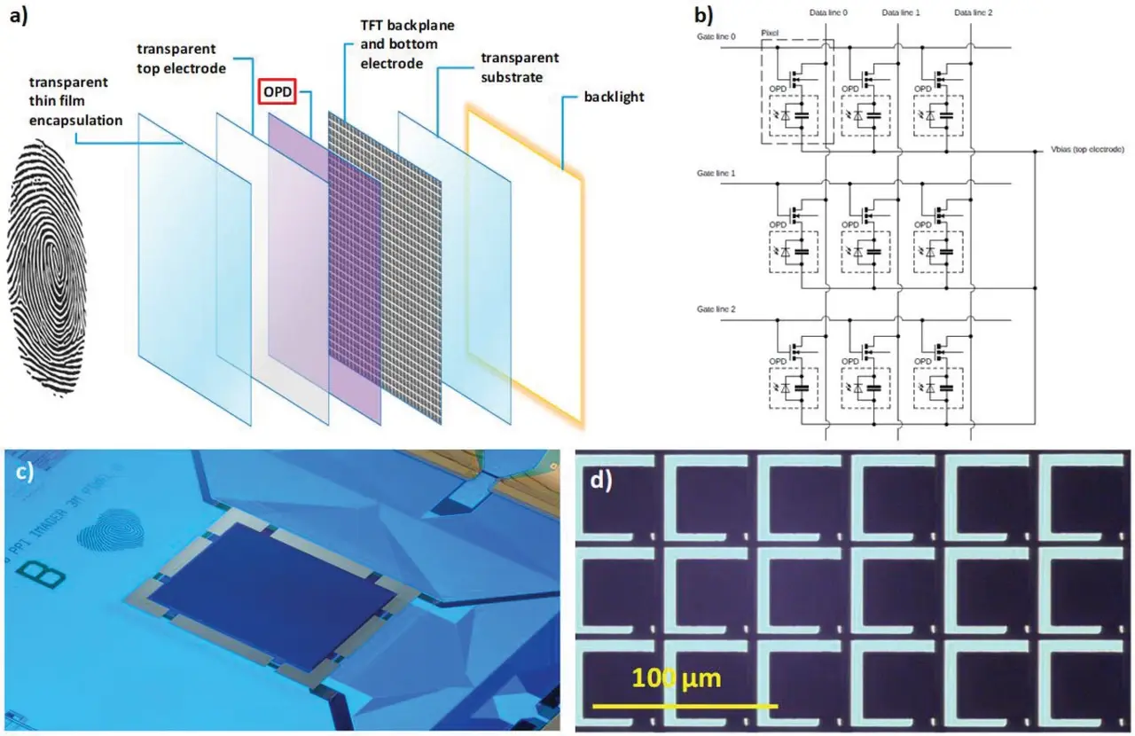
Figure 1
a) Schematics of the reflective fingerprint scanner. The imager consists of a backlight, an a‐IGZO thin‐film transistor (TFT) backplane, a bulk heterojunction (BHJ) OPD frontplane, and a thin‐film encapsulation barrier. Light goes through the semitransparent area of the imager, it is then reflected by the finger and detected by the OPD pixels. b) Circuit diagram of the fingerprint scanner. c) Photograph of the full fingerprint sensor. d) Transmission microscopy image of a part of the pixel array of the image sensor (6 × 3 pixels).
The sensor has a resolution of 508 pixels per inch (ppi)—the FBI standard for fingerprint authentication.16, 17 It comprises 640 × 480 pixels (resulting in a total sensor size of 3.2 × 2.4 cm). As mentioned, the BHJ OPD solution is deposited by slot‐die coating. Slot‐die coating is used as it produces homogeneous films with well‐controlled layer thickness over large area. To check this, the layer thickness of the BHJ OPD was measured by profilometry over 15.2 × 15.2 cm glass plates. We obtained highly uniform films (280–300 nm) with a variation of less than ≈7% (20 nm). The OPD is not patterned and the active pixel area is therefore set by the bottom electrode on the TFT backplane. The pixel size is 50 × 50 µm, with an active area of the pixel of 920 µm2 or 37% of the total surface (see Figure S2, Supporting Information, for a schematic view of the pixel array). A commercial white LED smartphone backlight is used as a light source. The working principle is as follows: Light is emitted from the LED backlight and is transmitted through the semitransparent areas of the array (see light areas in Figure 1d) hitting the target (e.g., a finger) and bouncing back to the OPD, where light is detected and data are processed to obtain a full grayscale image (e.g., a fingerprint). In order to achieve this, it is paramount that a sufficient amount of light traverses the full device. Figure 1d is a bottom‐illuminated microscope image showing the semitransparent areas (in light blue) where the light is transmitted. The darker parts are covered with the opaque bottom electrode materials. The lighter areas comprise 26% of the full surface of the TFT backplane. As the frontplane is not patterned, part of the light is also absorbed by the different layers (BHJ OPD, electrodes, TFE) through these openings. The resulting transmitted light through the full fingerprint sensor is less than 7% for any wavelength across the visible spectrum (Figure S3, Supporting Information). Despite this low transmission, the OPD is capable of imaging a fingerprint or any other object placed on top, even using a backlight at low brightness (<1 cd m−2). To detect these low light levels, it is required that the OPD performance excels on the photodetector key parameters (dark current, responsivity, detectivity), which are characterized in the next section.
OPD test devices having the same layer structure and processing conditions as the OPD frontplane were fabricated to measure the OPD performance. These consisted of a series of 1 mm2 pixels. The electrical performance of the photodiodes was characterized on 49 different devices (1 mm2). A characteristic J–V curve (−2 to 2 V) of one of the pixels is presented in Figure 2a, both in dark (blue line) and under light (red line). The J–V curves have no hysteresis and behave as excellent diodes, as they show a dark current rectification ratio of more than 106 in the −2 to 2 V range with a very sharp current increase at low, positive voltages. The devices were driven continuously at −2 V to extract the steady‐state dark current (Figure 2a, inset). The median extracted reverse bias current density (of the 49 OPDs) is 9.9 × 10⁻⁸ mA cm−2 at −2 V (Figure 2b). A low dark current indicates that the OPDs can work even with low levels of light. These values are comparable to a‐Si based photodiode devices,18 and among the lowest reported for OPDs in literature.1 The dark current was lowered by carefully choosing blocking layers that effectively limit the injection of charge carriers through the electrodes, in this case MoOx and a‐IGZO.19 A different approach has been previously used to lower the dark current on the same BHJ OPD system (PCDTBT:PCBM), namely, the use of a polyethylenimine ethoxylated (PEIE) layer to reduce the work function of the electrode. For instance, Kielar et al. obtained dark currents of 7.6 × 10⁻³ mA cm−2 which were optimized by incorporating PEIE down to 2.7 × 10⁻⁷ mA cm−2.20 Pierre et al. also used PEIE on top of the cathode and reported devices with dark currents of 1.5 × 10⁻⁷ mA cm−2 at −5 V.21 The J–V under a microscope light (Figure 2a) had a median current density of 4.2 × 10⁻¹ mA cm−2 at 2 V (Figure 2b), The current density increases more than six orders of magnitude and shows little voltage dependence, an indication of the very good charge extraction capabilities of these devices. The external quantum efficiency (EQE) and spectral responsivity (SR) were measured (Figure S4, Supporting Information). The EQE measures the photosensitivity of the device and was measured under a constant voltage of −2 V. The OPD blend has a maximum EQE of ≈50% at 550 nm, and it is above 40% on the 470–600 nm range. The optical absorption onset is around 700 nm. The spectral responsivity of the OPD has a value of 0.21 A W−1 at 580 nm. The specific detectivity was calculated (Figure 2c), resulting in a detectivity of 7.1 × 10¹³ Jones at 580 nm and under a −2 V bias. Finally, the linearity was characterized (Figure 2d). Linearity is important for a fingerprint sensor as the lighting (both ambient and backlight) can change in different operation conditions. The results show that the OPD behaves linearly (R‐square of 0.99999) with current density values ranging from 1.6 × 10⁻³ to 1.3 × 10⁻² mA cm−2 for light intensities ranging from ≈30 to 235 µW cm−2, respectively. Overall, the OPD stack presents high performance in the characterized figures of merit.
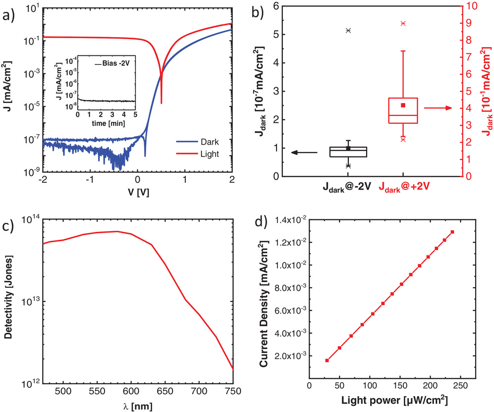
Figure2
a) J–V characteristics of the BHJ OPD in dark (blue curve) and under light (red curve). Inset: Current density under dark versus time at a constant bias of −2 V. b) Box plots of dark current at reverse bias (−2 V, black, left axis) and at forward bias (2 V, red, right axis). The box is determined by the 25th and 75th percentiles, the lines determine the median values, and the squares the average values. The whiskers determine the 5th and 95th percentiles. Small crosses determine the 1st and 99th percentiles. Small lines determine the maximum and minimum values. c) Detectivity of the BHJ OPD at −2 V. d) Linearity (current density vs light power) of the BHJ OPD.
The current density was also measured as a function of luminance (Figure 3a). There is a linear response up to 5 cd m−2 (R‐square = 0.99), with current densities ranging from 4.6 × 10⁻⁵ to 6.2 × 10⁻⁴ mA cm−2 for light intensities ranging from around 0.25 to 5.0 cd m−2, respectively, after which the current saturates as a result of the depletion of charges on the pixels, which can be increased by increasing the bias voltage and the readout setting of the peripheral electronics in general. From the readout charge at the plateau values, the saturation charge is 0.3 pC (using a bias voltage of 3 V). Likewise to the linearity of the OPD, in the full device also the linear response allows an operation in a wide range of light intensities, including very low light level intensities. Next, the pixel current density of all the pixels of the array (640 × 480 pixels) was measured in dark and under a light exposure of ≈3.5 cd m−2, in the linear range (Figure 3b). Both dark and light response follow a gaussian shape and show a narrow distribution, an indication of high uniformity. The dark response was offset‐corrected, pixels with negative current density correspond to nonfunctional pixels which originally were at zero. The light response gaussian shape has a x c of 4.79 × 10⁻⁴ mA cm−2 and an R‐square of 0.999. When a fingerprint (or other object) is captured the quality of the image can be enhanced by offset correction and gain correction for each pixel (Figure S5a, Supporting Information). In this case, the resulting distribution of pixels is much narrower, virtually all the pixels show the same intensity (Figure S6b, Supporting Information).
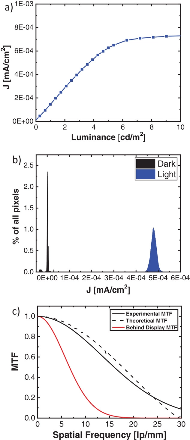
Figure3
a) Pixel current density as a function of luminance for the image sensor. b) Histogram of the pixel current density of the image sensor in dark (black) and under light (blue). c) MTF as a function of spatial frequency with an LED source located at >1 m distance (solid black line), an OLED on top of the imager (solid red line) as well as the theoretical expected value (dashed black line).
The spatial resolution of the image sensor was quantified using the so‐called modulation transfer function (MTF): The contrast over a series of line pairs (transparent/nontransparent) was tested over different line spacings. This was measured by using the slanted‐edge method22 by placing an LED light source at a far distance to guarantee perpendicular light. Figure 3c shows the obtained MTF curve (solid black line). The MTF20 (minimum value where two lines can be visually resolved) is 24.3 lp mm−1. The theoretical MTF (dashed black line) is also plotted showing very good agreement with the experimental results.
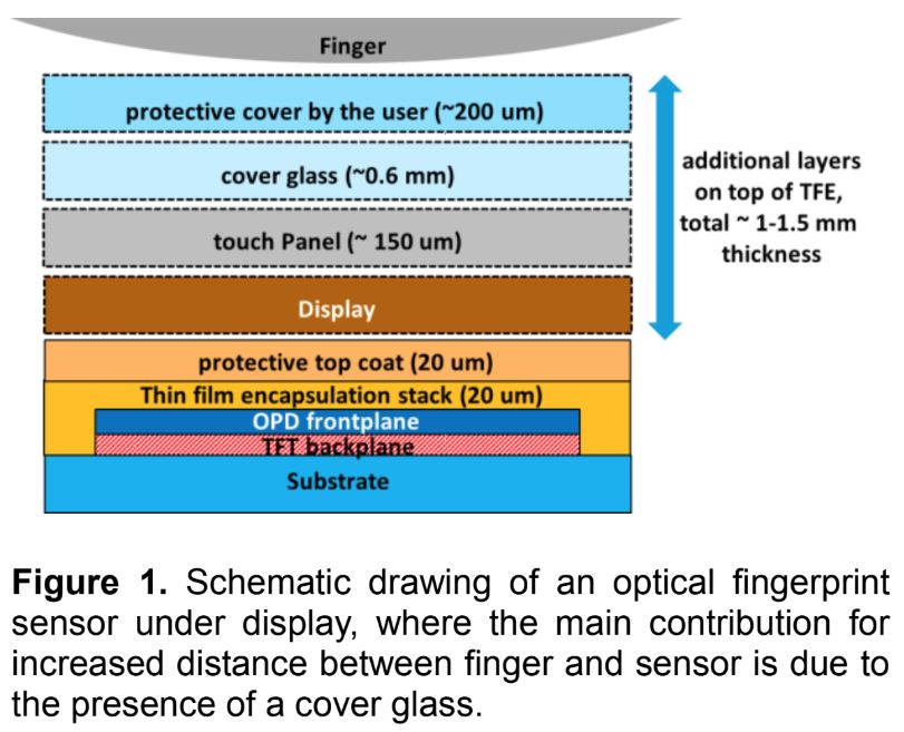
When implemented behind a display, the source of light is the display itself. In this setup, not all the incoming light is “collimated” perpendicular and the MTF is expected to be reduced. This was mimicked by placing an OLED tile directly on top of the imager. The resulting MTF is also shown in Figure 3c (solid red line). In this configuration, the MTF20 is 10.0 lp mm−1. Placing a thick protection layer or a display (mimicking under‐display optical fingerprint applications) on top of the sensor increases the distance between the sensor and the finger, promoting pixel cross‐talk and thus decreasing the resolution of the fingerprint (or object) even more. In order to prevent resolution loss, the encapsulation should be made thin. On the other end, the OPD materials should also be protected from moisture from the ambient. Holst Centre has developed a state‐of‐the‐art thin film encapsulation stack, consisting of SiN layers, separated by an organic coating.23 This encapsulation stack ensures long lifetime and with a thickness of around 40 µm does not negatively impact the overall resolution of the imager. Indeed, the dark current of encapsulated test devices was measured, showing that the dark current values remain constant, even after more than 400 d (Figure S6, Supporting Information). Likewise, the current density as a function of luminance for the full array was measured at different points in time, showing almost identical curves over a timespan of 175 d (Figure S7, Supporting Information).
Finally, we captured fingerprints in reflection mode by using a backlight illumination. Figure 4 shows the fingerprint raw image (Figure 4a) and the image after offset/gain correction and interpolation of dead pixels (Figure 4b), corrections that clearly increase the contrast and definition of the image. The fingerprint image quality can be defined by how the system is able to resolve biometric parameters classified at three levels of detail: deltas and cores (level 1), ridge bifurcations and endings (level 2), and pores (level 3).24 Images obtained with the fingerprint sensor in this work are able to resolve level 3 details, as it is shown by Figure 3c, where the sweat pores are clearly visible on top of the ridges. A cross‐sectional image along the center of a fingerprint shows good contrast of around 7000 least significant bits (LSB) between the valleys (darker regions, ≈27 000 LSB) and the ridges (lighter regions, ≈34 000 LSB) of the fingerprint, as shown in Figure S8 (Supporting Information) (the absolute LSB levels are tunable depending on the settings of the hardware and the brightness of the light source). This provides quantitative data for accurate fingerprint recognition.24 The frame rate used is 35 fps, showing the possibility of using the image sensor for applications where fast response is needed. When using a backlight behind the sensor, light goes through the semitransparent area of the imager, it is then reflected by the fingerprint and detected by the OPD pixels. The quality of the image decreases with increasing distance of the finger to the detector, in this particular case the distance is determined by the thickness of the encapsulation of ≈40 µm, hence the importance to have a very thin film encapsulation layer while keeping sufficient barrier properties, as mentioned. The backlight is not directly detected by the OPD pixels as an opaque shielding bottom electrode is used. Low light levels of <1 cd m−2 can be used due to a combination of the pixel aperture of the imager, the low dark current, and high responsivity of the OPD. Integrating the image sensor under display is also possible by placing the display on top of the sensor and using the own display as a light source. In this way, the image sensor could be implemented into smartphones and tablets for full‐display‐area fingerprint recognition. We believe future development of this technology should focus on the improvement of the EQE that can be achieved by a more transparent top electrode which will result in a higher contrast of the fingerprint images, higher resolution of the arrays, and patterning of the OPD active material.
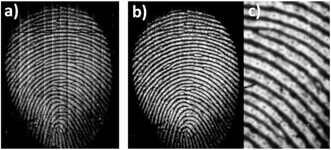
Figure4
a) Fingerprint image obtained with the image sensor. b) Fingerprint image after offset/gain/nonfunctional pixel correction. c) Close‐up of (b), where pores are clearly visible.
Summarizing, we have developed an optical fingerprint scanner using a slot‐die coated OPD frontplane and an a‐IGZO DG‐SA TFT backplane. The imager consists of 640 × 480 pixels with a resolution of 508 ppi. The imager can be operated in reflection mode by incorporating a backlight or partially transparent display on top. The OPDs show excellent performances with dark currents below 1 × 10⁻⁷ mA cm−2, linearity over a wide range of light intensities, and a detectivity of 7.1 × 10¹³ Jones. The imager has a high spatial resolution, close to the expected value due to the thin‐film encapsulation used, and a large dynamic range. The uniformity is high, with pixels showing a narrow current distribution both in dark and under light. The imagers are stable over time, with a response of the pixels that is the same after more than a year of storage. High‐resolution images of fingerprints are obtained by using a backlight as the light source. All processing is compatible with flat panel display manufacturing lines. Thus, the imager can potentially be upscaled very cost‐effectively to very large sizes. Its thin form factor enables seamless integration in standalone biometric applications, for mobile phones, and access security.
Experimental Section
Imager Sensor Fabrication : The full stack cross section is shown in Figure S1 (Supporting Information). The processing is as follows. First, a polyimide precursor (DuPont) was deposited on the glass carrier (Corning Inc.) and cured, after which a polyimide foil with a thickness of 15 µm is obtained. Then, a 100 nm SiNx layer was deposited by plasma‐enhanced chemical vapor deposition (PECVD) forming the bottom encapsulation barrier. 130 nm Mo‐alloy (JX Nippon) bottom gate electrode was sputtered and patterned using wet etching. A 200 nm SiO2 was then deposited by PECVD as bottom gate insulator. IGZO (JX Nippon) was sputtered at room temperature with a metal ratio of 1:1:1. The IGZO was patterned by wet etching. Another 200 nm SiO2 was deposited by PECVD, as top gate insulator. Then 130 nm of Mo‐alloy was deposited as top gate metal. The SiO2 and the MoCr layers were patterned by wet etching followed by dry etching. Then a 200 nm SiN layer was deposited by PECVD as intermetal dielectric. This decouples the top gate and source–drain metal layers and dopes the IGZO in the areas that are not covered by the top‐gate stack (forming a homojunction between the doped IGZO contact region and the IGZO channel). Then via holes were created in the intermetal dielectric by dry etching, in order to contact the IGZO and the top gate metal. This was followed by another dry etching step in order to create via holes to contact the bottom gate metal. Then a source–drain 130 nm layer of MoCr was sputtered and patterned by wet etching. A post‐TFT fabrication anneal at 165 °C was performed. Next, an organic material interlayer (TOK) was coated and structured by photolithography and development. Another 130 nm MoCr‐alloy bottom pixel electrode was deposited and patterned, as well as the ETL (IGZO) was sputtered and patterned by wet etch. An edge cover/pixel definition layer was deposited and photolithographically structured (exposure + development) to define the OPD active layer. The polymer PCDTBT (PCAS) and PCBM (nano‐c) were weighted in a 1:4 ratio and dissolved in chlorobenzene. The solution was stirred at 90 °C overnight. The active layer (280 nm) was then deposited by slot‐die coating and then annealed for 15 min at 60 °C. The HTL and anode layers (both purchased at Alfa Aesar) were deposited by thermal evaporation. A transparent thin film encapsulation stack was applied by PECVD and inkjet printing, having a water vapor transmission rate (WVTR) ≪ 10−6 g m−2 d−1.23 The gate drivers and readout ICs were bonded to the fan‐out electronics. The driving and readout hardware was developed in‐house. Test devices were also fabricated. Glass sheets were used as the substrate. The process is the same as the aforementioned, starting by the MoCr‐alloy bottom pixel electrode.
OPD Characterization : OPD test devices were characterized in a glovebox under a N2 atmosphere and at ambient temperature. Current versus voltage characteristics were measured using an Agilent 4155C semiconductor parameter analyzer connected to manual probes. External quantum efficiency was also measured in a glovebox under a N2 atmosphere and at ambient temperature. The system uses a solar simulator light source and a series of filters resulting in 20–50 nm steps.
Image Sensor Characterization : Microscope images were obtained using a Leica DM2500M microscope. MTF was characterized by using a standard negative resolution target R2L2S1N1 (Thorlabs). An LED located at >1 m distance and an OLED tile in close contact were used as light sources. The MTF was extracted by using the slanted‐edge method (ISO 12233 Standard compliant)22 with a custom‐made LabVIEW program. Light‐intensity measurements were obtained by using an OLED tile light source, previously calibrated and measuring the response at different light intensities. The response was averaged over ten full sensor images. Response of pixels under dark and under light as well as the offset/gain correction and interpolation of dead pixels were carried out by using a custom‐made LabVIEW program and the aforementioned OLED tile as the light source. The response was also averaged over ten full sensor images. Fingerprint images were obtained by using a backlight and measuring the response, with a frame rate of 35 fps. The fingerprint was captured from a live subject.
Acknowledgements
The authors would like to thank the process engineers of Holst Centre's R&D TFT Pilot Line for the realization of the TFT backplanes, as well as the thin‐film encapsulation on top of the OPD frontplane. This work was partly financed through the Flexlines project within the Interreg V‐programme Flanders‐The Netherlands, a cross‐border cooperation programme with financial support from the European Regional Development Fund, and co‐financed by the Province of Noord‐Brabant, The Netherlands.
Conflict of Interest
The authors declare no conflict of interest.
p.s
imec/Holst Centre, organic film image sensors
blog.daum.net/serapeum/7594916
화면 1/2 영역과 전화면 지문인식을 위한 Organic TFT기반 지문인식
blog.daum.net/serapeum/7595000
위 논문은 640×480 pixels (total sensor size of 3.2 × 2.4 cm) @508 dpi.
아래 imec 의 자료 92.4 x 110.9 mm2, 500dpi, 70% transparency in the visible region
이 기술이 주목받는 이유는 투명하고 휘어지는 특징때문이고 응용시장이 크기 때문이다. X-Ray기기에도 응용가능하다.